- 您现在的位置:买卖IC网 > Sheet目录346 > NCP5680MUTXG (ON Semiconductor)IC LED DRIVER WHT HI EFF 24-UQFN
�� �
�
�NCP5680�
�Select� FlashTrigger�
�CONFIG1[EXTRG)�
�I2C� TRIGGER� Selected�
�External� Trigger� Selected�
�I2C� TRIGGER� Selected�
�Set� I2CTRIG�
�Set� TimeOut�
�Send� EXTLTRIGGER�
�Read� Flash� Pulse�
�The� Flash� duration� is� setup� by�
�the� I2C� FLWIDx� register�
�The� Flash� duration� is� equal� to�
�the� EXTL� TRIGGER� Pulse� width�
�The� Flash� is� switched� OFF� by�
�the� Time� Out� control�
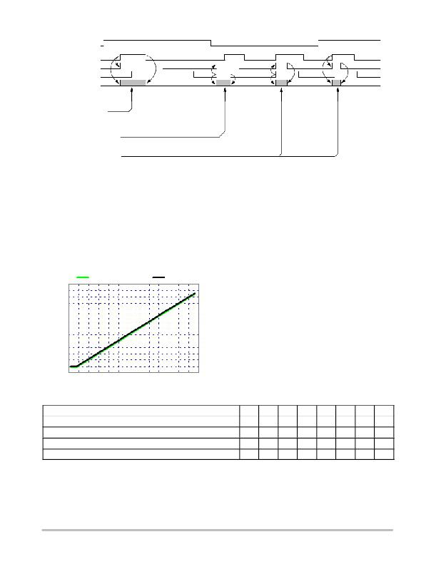
�Figure� 12.� Flash� Mode� of� Operation�
�When� the� power� flash� is� activated,� the� default� Time� out�
�is� preset� to� 50� ms� typical� and� can� be� set� up� to� a� different�
�timing� through� an� I2C� command.� Although� the� NCP5680�
�can� sustain� a� 255� ms� time� out,� care� must� be� observed,� at�
�system� level,� that� both� the� external� NMOS� transistors� and�
�the� LED� are� capable� to� absorb� the� increase� of� temperature�
�coming� from� the� extra� heat� developed� during� a� larger� time�
�out� sequence.�
�LED� Flash� Current� @� Vbat=3.6V�
�LED1 LED2�
�700�
�650�
�600�
�550�
�500�
�450�
�400�
�350�
�300�
�250�
�200�
�150�
�100�
�Flash� Configuration�
�To� generate� a� flash� pulse,� several� registers� must� be� preset�
�before� a� flash� takes� place:�
�FILED1� =� $03� 3� LED1� set� up� the� peak� current�
�FILED1� =� $04� 3� LED2� set� up� the� peak� current�
�FLDLY1� =� $07� 3� LED1� set� up� the� delay� time�
�FLDLY2� =� $08� 3� LED2� set� up� the� delay� time�
�FLWID1� =� $0A� 3� LED1� set� up� the� pulse� width� time�
�FLWID2� =� $0B� 3� LED2� set� up� the� pulse� width� time�
�VOUTREG� =� $0F� 3� set� up� the� output� voltage� value�
�TOUT� =� $14� 3� set� up� the� time� out�
�A� typical� sequence� is� depicted� here� below:�
�?� Set� up� the� configuration� registers� to� control� the� flash�
�sequence�
�?� Set� up� the� pulse� width,� the� amplitude� and� the� delay�
�time�
�50�
�0�
�0.0 0.5 1.0 1.5 2.0 2.5 3.0 3.5 4.0 4.5 5.0 5.5 6.0 6.5�
�FILED(A)�
�Figure� 13.� Flash� ILED� Current� vs.� Vsense�
�CONFIG0�
�Select� the� Photo� Sense� Mode� of� Operation�
�Select� the� Automatic� LED� check� during� a� pulse�
�Select� LED2�
�Select� LED1�
�B7�
�?�
�?�
�?�
�?�
�B6�
�?�
�?�
�?�
�?�
�B5�
�1/0�
�?�
�?�
�?�
�B4�
�?�
�1/0�
�?�
�?�
�B3�
�?�
�?�
�?�
�?�
�B2�
�?�
�?�
�?�
�?�
�B1�
�?�
�?�
�1/0�
�?�
�B0�
�?�
�?�
�?�
�1/0�
�Typical� Sequence:�
�?� send� the� I2C� address�
�?� select� the� CONFIG0� register�
�?� activate� LED1� and� LED2�
�$7C�
�$01�
�$03�
�http://onsemi.com�
�17�
�发布紧急采购,3分钟左右您将得到回复。
相关PDF资料
NCP5890MUTXG
IC LED DRVR WHITE BCKLGT 16-UQFN
NCP5901BMNTBG
IC MOSFET DVR SYNC VR12 8-DFN
NCP5901MNTBG
IC MOSFET DVR SYNC VR12 8-DFN
NCP5911MNTBG
IC MOSFET DVR SYNC VR12 8-DFN
NCP692MN50T2GEVB
EVAL BOARD FOR NCP692MN50T2G
NCV7513AFTR2G
IC PREDRIVER HEX LOW SIDE 32LQFP
NCV7513BFTR2G
IC PREDRIVER HEX LOW SIDE 32LQFP
NCV7513FTG
IC PREDRIVER HEX LOSIDE 32-LQFP
相关代理商/技术参数
NCP571
制造商:ONSEMI 制造商全称:ON Semiconductor 功能描述:150 mA CMOS Low Iq Low Output Voltage Regulator
NCP57152
制造商:ONSEMI 制造商全称:ON Semiconductor 功能描述:1.5 A, Very Low-Dropout (VLDO) Fast Transient Response Regulator
NCP57152DSADJR4G
制造商:ON Semiconductor 功能描述:1.5A ADJ VLDO REGULATOR - Tape and Reel 制造商:ON Semiconductor 功能描述:1.5A ADJ VLDO REGULATOR - Cut TR (SOS) 制造商:ON Semiconductor 功能描述:REEL / 1.5A ADJ VLDO REGULATOR
NCP57152MNADJTYG
制造商:ON Semiconductor 功能描述:1.5A ADJ VLDO REGULATOR - Tape and Reel 制造商:ON Semiconductor 功能描述:1.5A ADJ VLDO REGULATOR - Cut TR (SOS) 制造商:ON Semiconductor 功能描述:REEL / 1.5A ADJ VLDO REGULATOR
NCP571MN08TBG
功能描述:直流/直流开关转换器 LDO RoHS:否 制造商:STMicroelectronics 最大输入电压:4.5 V 开关频率:1.5 MHz 输出电压:4.6 V 输出电流:250 mA 输出端数量:2 最大工作温度:+ 85 C 安装风格:SMD/SMT
NCP571MN08TBGEVB
功能描述:BOARD EVAL NCP571MN 0.8V RoHS:是 类别:编程器,开发系统 >> 评估板 - 线性稳压器 (LDO) 系列:* 产品变化通告:1Q2012 Discontinuation 30/Mar/2012 设计资源:NCP590MNDPTAGEVB Gerber Files 标准包装:1 系列:- 每 IC 通道数:2 - 双 输出电压:1.8V,2.8V 电流 - 输出:300mA 输入电压:2.1 ~ 5.5 V 稳压器类型:正,固定式 工作温度:-40°C ~ 85°C 板类型:完全填充 已供物品:板 已用 IC / 零件:NCP590MNDP 其它名称:NCP590MNDPTAGEVB-NDNCP590MNDPTAGEVBOS
NCP571MN09TBG
功能描述:低压差稳压器 - LDO LDO BUS SWTCH RoHS:否 制造商:Texas Instruments 最大输入电压:36 V 输出电压:1.4 V to 20.5 V 回动电压(最大值):307 mV 输出电流:1 A 负载调节:0.3 % 输出端数量: 输出类型:Fixed 最大工作温度:+ 125 C 安装风格:SMD/SMT 封装 / 箱体:VQFN-20
NCP571MN09TBGEVB
功能描述:BOARD EVAL NCP571MN 0.9V RoHS:是 类别:编程器,开发系统 >> 评估板 - 线性稳压器 (LDO) 系列:* 产品变化通告:1Q2012 Discontinuation 30/Mar/2012 设计资源:NCP590MNDPTAGEVB Gerber Files 标准包装:1 系列:- 每 IC 通道数:2 - 双 输出电压:1.8V,2.8V 电流 - 输出:300mA 输入电压:2.1 ~ 5.5 V 稳压器类型:正,固定式 工作温度:-40°C ~ 85°C 板类型:完全填充 已供物品:板 已用 IC / 零件:NCP590MNDP 其它名称:NCP590MNDPTAGEVB-NDNCP590MNDPTAGEVBOS